Microfluidic on CMOS with Laser Cut Adhesive Tape

ty10086 提交于 周四, 08/26/2021 - 13:03
文章英文标题
Microfluidic on CMOS with Laser Cut Adhesive Tape
正文
CMOS integrated circuits are an ideal platform for microfluidic-based sensing because they offer small feature size at low cost and can incorporate control and sensing circuitry\u003csup\u003e1\u003c/sup\u003e.Fabricating microfluidic devices on top of CMOS presents two challenges: bonding the channel to the CMOS surface and working with the small area that is usually available. This paper presents and compares two techniques for building microfluidic networks on CMOS.;\u003cbold\u003eObjectives \u003c/bold\u003e;The goal of this project is develop an efficient way of prototyping microfluidic devices on CMOS that can be translated into production.;\u003cbold\u003eNew Results\u003c/bold\u003e;Poly(dimethylsiloxane) (PDMS) has been widely used for making microfluidic devices on glass substrates\u003csup\u003e1\u003c/sup\u003e. Conventional microfluidic devices are formed by pouring uncured PDMS over a master. The cured slab is the peeled off from the master to punch ports and laid on a glass slide. The chamber is bonded by exposing the slide to oxygen plasma\u003csup\u003e2\u003c/sup\u003e. This technique works when the sample is analyzed under a microscope, but cannot be used on a CMOS chip.;In this work, this technique was modified by using uncured PDMS as a glue to bond the cured PDMS chambers to the CMOS. To make the device, the cured chamber with punched ports was placed on the sensor and held down to hold it in place for a few seconds. Uncured PDMS was deposited on the outer edges of the channel so that the bottom of the channel is a clean CMOS sensor. The PDMS was then flash cured with a hot air gun. Tubing was then inserted at the ports before imaging. This set up was capable of imaging fluorescence sample but fabrication could not be consistently repeated. Images of the master, chamber, and the imager is shown in Fig 1.;For the second method, Pressure Sensitive Adhesive (PSA) tape was used to make the microfluidic device\u003csup\u003e3\u003c/sup\u003e. For testing, we used a CO\u003csub\u003e2 \u003c/sub\u003elaser to cut the microfluidic channels out of the tape. The tape defines a channel which is 46.26 µm. In production, a die cutting process could be used. For conventional microfluidic device, the tape was stuck on a glass slide and the top layer was formed by placing a piece of clear acrylic plastic or a slab of PDMS. The thickness of the top layer serves to hold the inlet and outlet tubing. We have observed that PDMS forms a tighter seal around the tubing than acrylic plastic.;When working on CMOS chips, the tape was stuck to the sensor and then the punched PDMS slab was placed on top to seal the chamber. Apart from occasional leaks at the input and output ports, acrylic plastic also filtered most of the UV light during fluorescence imaging. An image of the PDMS, PSA tape, and the imager is shown in Fig 2.;Figure1: Microfluidic device made from PDMS (A) Master made from copper plates (B) Cured PDMS microfluidic chamber (C) Sealed chamber on CMOS imager;Figure2: Microfluidic device made from PSA tape (A) Top layer made of PDMS (B) Patterned PSA tape (C) Sealed chamber on CMOS imager;\u003cbold\u003eConclusion\u003c/bold\u003e;This microfluidic fabrication technique is repeatable and can be used to make microfluidic chambers with any dimensions and patterns. These on-sensor lensless imaging devices can be used for sample detection during fluorescence imaging and white light imaging, studying sample interaction, fluid dynamics, and for implementation of a low cost, portable, flow cytometer.;\u003cbold\u003eReferences\u003c/bold\u003e;1 D Psaltis, S Quake, C Yang, “Development optofluidic technology through the fusion of microfluidics and optics”, Nature, Vol 442, 2006;2 J Friend, A Yeo, “Fabrication of microfluidic device using polydimethylsiloxane”, Biomicrofluidics, 4, 2010;3 T Merian, F He, H Yan, D Chu, J Talbert, J Goddard, S Nugen, “Development and surface characterization of an electrowetting valve for capillary-driven microfluidics”, Colloids and Surfaces A: Physiochem. Eng Aspects 414, pp. 251-258, 2012;[Formula]
文章内容(英文)
CMOS integrated circuits are an ideal platform for microfluidic-based sensing because they offer small feature size at low cost and can incorporate control and sensing circuitry\u003csup\u003e1\u003c/sup\u003e.Fabricating microfluidic devices on top of CMOS presents two challenges: bonding the channel to the CMOS surface and working with the small area that is usually available. This paper presents and compares two techniques for building microfluidic networks on CMOS.;\u003cbold\u003eObjectives \u003c/bold\u003e;The goal of this project is develop an efficient way of prototyping microfluidic devices on CMOS that can be translated into production.;\u003cbold\u003eNew Results\u003c/bold\u003e;Poly(dimethylsiloxane) (PDMS) has been widely used for making microfluidic devices on glass substrates\u003csup\u003e1\u003c/sup\u003e. Conventional microfluidic devices are formed by pouring uncured PDMS over a master. The cured slab is the peeled off from the master to punch ports and laid on a glass slide. The chamber is bonded by exposing the slide to oxygen plasma\u003csup\u003e2\u003c/sup\u003e. This technique works when the sample is analyzed under a microscope, but cannot be used on a CMOS chip.;In this work, this technique was modified by using uncured PDMS as a glue to bond the cured PDMS chambers to the CMOS. To make the device, the cured chamber with punched ports was placed on the sensor and held down to hold it in place for a few seconds. Uncured PDMS was deposited on the outer edges of the channel so that the bottom of the channel is a clean CMOS sensor. The PDMS was then flash cured with a hot air gun. Tubing was then inserted at the ports before imaging. This set up was capable of imaging fluorescence sample but fabrication could not be consistently repeated. Images of the master, chamber, and the imager is shown in Fig 1.;For the second method, Pressure Sensitive Adhesive (PSA) tape was used to make the microfluidic device\u003csup\u003e3\u003c/sup\u003e. For testing, we used a CO\u003csub\u003e2 \u003c/sub\u003elaser to cut the microfluidic channels out of the tape. The tape defines a channel which is 46.26 µm. In production, a die cutting process could be used. For conventional microfluidic device, the tape was stuck on a glass slide and the top layer was formed by placing a piece of clear acrylic plastic or a slab of PDMS. The thickness of the top layer serves to hold the inlet and outlet tubing. We have observed that PDMS forms a tighter seal around the tubing than acrylic plastic.;When working on CMOS chips, the tape was stuck to the sensor and then the punched PDMS slab was placed on top to seal the chamber. Apart from occasional leaks at the input and output ports, acrylic plastic also filtered most of the UV light during fluorescence imaging. An image of the PDMS, PSA tape, and the imager is shown in Fig 2.;Figure1: Microfluidic device made from PDMS (A) Master made from copper plates (B) Cured PDMS microfluidic chamber (C) Sealed chamber on CMOS imager;Figure2: Microfluidic device made from PSA tape (A) Top layer made of PDMS (B) Patterned PSA tape (C) Sealed chamber on CMOS imager;\u003cbold\u003eConclusion\u003c/bold\u003e;This microfluidic fabrication technique is repeatable and can be used to make microfluidic chambers with any dimensions and patterns. These on-sensor lensless imaging devices can be used for sample detection during fluorescence imaging and white light imaging, studying sample interaction, fluid dynamics, and for implementation of a low cost, portable, flow cytometer.;\u003cbold\u003eReferences\u003c/bold\u003e;1 D Psaltis, S Quake, C Yang, “Development optofluidic technology through the fusion of microfluidics and optics”, Nature, Vol 442, 2006;2 J Friend, A Yeo, “Fabrication of microfluidic device using polydimethylsiloxane”, Biomicrofluidics, 4, 2010;3 T Merian, F He, H Yan, D Chu, J Talbert, J Goddard, S Nugen, “Development and surface characterization of an electrowetting valve for capillary-driven microfluidics”, Colloids and Surfaces A: Physiochem. Eng Aspects 414, pp. 251-258, 2012;[Formula]
来源出处
Journal|[J]Meeting AbstractsVolume MA2014-01, Issue 40. 2014. PP 1500-1500

PDMS臻品推荐

PDMS-微流控基质材料-PDMS/道康宁SYLGARD184-聚二甲基硅氧烷/0.5KG(组)

产品说明书PDF自助在线看:http://www.pdmshub.com/sih

信息更新:

美国总工厂生产的0.5KG原始包装的PDMS延期至2021年9月16日后才能交货,默认我们将发国内库存的进口分装产品(02085925-0.5KG);另受制于有机硅大幅涨价潮影响,2021年9月1日后将上调销售价格,另行通知。Dow Corning=道康宁=Dow SiL=陶氏,都是同一家公司。 2021.09.01更新

美国总工厂生产的0.5KG包装的PDMS恢复正常进口,合法正规,质量金标准,欢迎订购使用。并承诺从我司购买的皆为原厂包装,100%未开封,附带技术手册,非国产灌装仿制、非分装、非仿冒外包装产品,可以放心使用。大量订购更有优惠。2021.04.01更新

备注:由于dowsil与道康宁公司合并,美国总工厂生产的PDMS,价格涨幅高达1倍之多,因针对科研用户使用,特备货规格0.5KG。如果您需要美国总工厂原厂生产的大规格包装的预定,可以与QQ 11366508联系给予报价/货期。2021.05更新

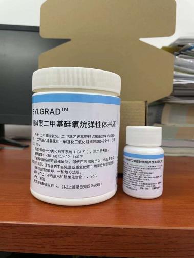
此链接为PDMS-微流控芯片/PDMS/道康宁SYLGARD184/小桶0.5KG装的链接。

一般性的产品性能参数表参考以下小桶装的参数:

微流控芯片/PDMS/道康宁SYLGARD184;微流控芯片/PDMS/道康宁SYLGARD184;微流控芯片/PDMS/道康宁SYLGARD184;

品牌型号:道康宁SYLGARD184

包装规格:0.5KG/罐[含有45.4g固化剂,总重量为0.5KG]

产品颜色:保质期限:36个月

存放环境说明:室温,阴凉处保存

备注说明:

美国道康宁道康宁SYLGARD 184硅橡胶是由液体组分组成的双组分套件产品,包括基本组分与固化剂。基本组分与固化剂按10:1重量比完全混合,中等粘度混合液的稠度与SAE 40机油相似。无论厚薄,混合液将固化成为具有韧性的透明弹性体,最适用于电子/电气方面的封装与灌封应用。 道康宁SYLGARD 184硅橡胶在25~150℃的温度范围内固化,无放热现象,无需二次固化。固化过程完成后,可立即在-55~200℃的温度范围内使用。 产品特性:低毒性,在常规的工业操作中,无特别的注意事项; 无溶剂或固化副产物, 固化时不放热;无需特殊的通风条件,不会产生腐蚀;固化时,收缩量小; 固化后, 透明具有弹性;抗震与减缓机械震动;振动的传递性能小;元件可裸视检查与易修补性; 环保性能;低吸水性,良好的耐辐射性能;高真空状态下的低漏气性; 优异的电性能;较大温度范围内的稳定性, 抗解聚;在-55~200℃范围内,甚至在密闭状态下保持弹性与柔韧性,性能稳定; 阻燃性,UL可燃性分级为94 V-1,温度等级:130℃ 产品用途: 道康宁SYLGARD 184硅橡胶在电气/电子的封装与灌封方面有广泛的应用。